1. Introduction
Traffic inside a data centre moves over optical links that are short by the standards of telecommunications, from a few metres to a few kilometres, and extremely numerous. Cost per lane, power per bit and density at the switch faceplate decide which technology is used, more than reach or spectral efficiency (Cheng et al., 2018). Silicon photonics entered this market because it builds waveguides, modulators and germanium photodetectors on wafers processed in foundries designed for electronics, with the yield and volume that follow (Thomson et al., 2016).
Within such a transceiver the modulator carries a particular burden. The laser can be a simple continuous wave source and the photodetector has bandwidth to spare, so the modulator and its driver set the symbol rate, a good part of the power budget and much of the chip area. The Ethernet standard for 400 Gb/s adopted four level pulse amplitude modulation, with lanes of 100 Gb/s in the 500 m variant (IEEE, 2017), and later generations ask for still higher symbol rates. Each step tightens the requirements on the modulator.
Miller (2009) set out early what an optical interconnect device would have to achieve to compete with copper close to the chip, and stressed energy per bit as the governing figure. This review takes up the same concern from the side of the device. It asks what the published work says about three limits, bandwidth, drive voltage and packaging, and how far they can be moved.
2. Scope and Approach
This is a narrative review of the published literature. It draws on landmark device papers, on earlier reviews of silicon modulators (Reed et al., 2010; Witzens, 2018; Rahim et al., 2021) and on reviews of photonic packaging. No systematic search was carried out and no claim of completeness is made. The selection favours work that explains a limit over work that reports a record. Performance figures are described qualitatively except where a value is a matter of standard or definition, because published records depend on measurement conditions that differ from one laboratory to another.
3. Physical Basis of Modulation in Silicon
Crystalline silicon is centrosymmetric, so the linear electro-optic, or Pockels, effect that serves lithium niobate modulators is absent in the unstrained material. The useful mechanism is the plasma dispersion effect: a change in the density of free electrons and holes changes both the refractive index and the absorption. Soref and Bennett (1987) quantified the effect at the telecommunication wavelengths, and their empirical relations are still the starting point of device design. Two consequences follow directly. The index change is small, so long interaction lengths or resonant enhancement are needed, and phase modulation is always accompanied by a change in loss.
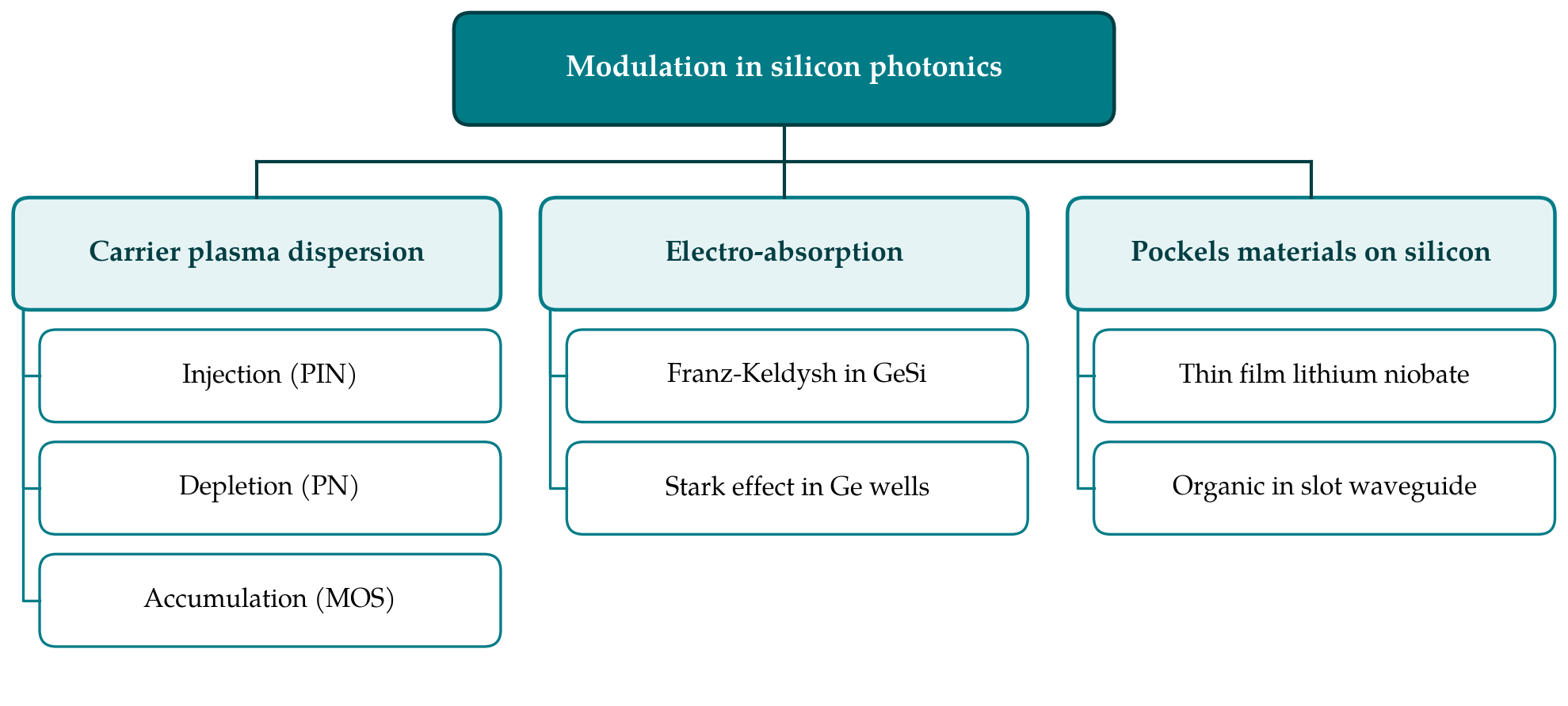
Three electrical structures move carriers in and out of the optical mode, and Figure 1 places them within the wider family of modulation mechanisms available on the platform. Carrier injection in a forward biased PIN diode gives a large index change at low voltage, but its speed is held back by the recombination lifetime of minority carriers unless the drive signal is pre-emphasised (Xu et al., 2005; Green et al., 2007). Carrier accumulation on either side of a thin oxide, as in the device of Liu et al. (2004) that first exceeded 1 GHz in silicon, is fast but capacitive. Carrier depletion in a reverse biased PN junction is the fastest and has become the standard choice, at the price of a weaker effect per volt (Liao et al., 2007).
4. Bandwidth
The electro-optic bandwidth of a depletion modulator is set by different things in a long device and in a compact one. In a Mach-Zehnder modulator the phase shifters are millimetres long, comparable with the wavelength of the microwave drive, and are built as travelling wave electrodes. Bandwidth is then limited by three effects treated at length by Witzens (2018): microwave loss along the electrode, which is dominated by the series resistance of the doped silicon that connects the metal to the junction; mismatch between the velocity of the microwave and the group velocity of the light; and mismatch between the line impedance and the driver.
The junction capacitance loads the transmission line, slowing the microwave and lowering its impedance, so the doping that strengthens modulation also degrades the line. Designers respond with segmented or slow wave electrodes, with substrate removal, and with lighter doping near the waveguide core, each of which trades against efficiency or optical loss. Depletion Mach-Zehnder modulators reached 50 Gb/s with simple on-off keying (Thomson et al., 2012), and later work has relied on multilevel formats and equalisation to carry higher rates through a similar analogue bandwidth (Rahim et al., 2021).
A microring modulator is tens of micrometres across and behaves as a lumped element. Its bandwidth has an electrical part, the product of junction capacitance and series resistance, and an optical part, the photon lifetime of the cavity (Bogaerts et al., 2012). A sharp resonance gives a large change in transmission for a small voltage but stores light for longer, so efficiency and speed pull in opposite directions through the quality factor. Operating the laser slightly off resonance can extend the response through optical peaking, at some cost in modulation depth and with a chirp that depends on the detuning.
5. Drive Voltage and Energy
The efficiency of a phase shifter is expressed as the product of the voltage needed for a phase shift of π and the length over which it is applied. For depletion devices in silicon this product is of the order of a volt centimetre, much weaker than for injection devices, so a Mach-Zehnder modulator driven at the voltages available from advanced CMOS, around one volt or below, would need to be impractically long and lossy. In practice the device is made a few millimetres long and driven with a swing of several volts from a dedicated driver, often in a silicon germanium bipolar process, or it is under-driven and the reduced optical modulation amplitude is accepted (Reed et al., 2010).
Energy per bit follows from the drive arrangement. A travelling wave electrode is terminated in a resistor and dissipates power continuously, whatever the data. A lumped device is charged and discharged, and its energy scales with capacitance and the square of the voltage swing, which is why compact resonant modulators have reported energies orders of magnitude below those of Mach-Zehnder devices (Dong et al., 2009; Timurdogan et al., 2014). Miller (2017) argued that reaching very low energies requires the modulator to sit close to its driver, since otherwise the capacitance of the interconnect dominates. The argument links drive voltage to packaging, taken up below. Table 1 summarises how the main device types compare on the properties discussed so far.
| Device type | Main strength | Main limit | Representative sources |
|---|---|---|---|
| Depletion Mach-Zehnder | Wide optical band, thermally tolerant | Length, drive swing, terminated power | Liao et al., 2007; Thomson et al., 2012 |
| Injection Mach-Zehnder | Strong effect at low voltage | Carrier lifetime limits speed | Green et al., 2007 |
| Microring, depletion | Small footprint, low energy | Narrow optical band, needs thermal control | Dong et al., 2009; Timurdogan et al., 2014 |
| GeSi electro-absorption | Compact, fast, no resonance | Fixed wavelength window, insertion loss | Liu et al., 2008; Kuo et al., 2005 |
| Lithium niobate on insulator | Pure phase modulation, low voltage | Separate material flow, device length | Wang et al., 2018 |
| Silicon-organic hybrid | Very strong electro-optic effect | Long term stability of polymers | Leuthold et al., 2013 |
6. Beyond the Plasma Effect
Because the limits above are rooted in the plasma dispersion effect itself, a second line of work adds other materials to the silicon platform. Germanium, already present for photodetectors, supplies electro-absorption. Liu et al. (2008) showed a waveguide integrated modulator using the Franz-Keldysh effect in a germanium silicon alloy, and Kuo et al. (2005) observed a strong quantum confined Stark effect in germanium quantum wells grown on silicon. Such devices are short and lumped, need no resonance, and have large bandwidth. Their drawbacks are an operating wavelength tied to the band edge of the alloy, which shifts with temperature, and appreciable insertion loss.
Materials with a Pockels effect remove the coupling between phase and loss. Thin films of lithium niobate bonded to an insulating substrate confine light tightly enough to bring the half wave voltage of a Mach-Zehnder modulator down to the level of CMOS drivers while keeping low optical loss (Wang et al., 2018). Electro-optic polymers placed in the slot of a silicon waveguide, the silicon-organic hybrid approach, give voltage length products far below those of depletion devices (Leuthold et al., 2013). Reviews agree that these routes outperform plasma dispersion as devices, and also that each adds process steps, materials and qualification work outside the established foundry flow (Rahim et al., 2021).
7. Packaging Limits
A modulator is useful only when light and microwaves can be brought to it, and the literature on packaging describes a set of constraints that are independent of the device physics (Carroll et al., 2016). The three that bear most directly on modulators are optical coupling, the electrical path from the driver, and temperature.
7.1. Optical coupling
The mode of a silicon wire waveguide is far smaller than that of a single mode fibre. Grating couplers diffract light out of the chip surface, allow testing on the wafer and tolerate relaxed alignment, but they are limited in optical bandwidth and sensitive to polarisation. Edge couplers with inverse tapers are broadband and nearly polarisation independent but need a prepared facet and tighter alignment (Marchetti et al., 2019). Every decibel lost at the couplers must be recovered by laser power or modulation amplitude, so coupling loss competes directly with the insertion loss and drive voltage of the modulator in the link budget.
7.2. The electrical path
At tens of gigahertz the connection between driver and modulator is part of the circuit. Wire bonds add inductance that peaks or rolls off the response, and flip chip bonding with micro bumps is preferred for its short and repeatable path (Carroll et al., 2016). The same reasoning has led the industry from pluggable modules at the faceplate towards co-packaged optics, in which the photonic chip shares a substrate with the switch circuit and the long lossy electrical trace across the board is removed (Margalit et al., 2021). For the modulator this shortens the path to the driver and so favours low capacitance lumped devices, but it also places the photonics in a hot and thermally unsteady environment and makes replacement in the field harder.
7.3. Temperature
Silicon has a large thermo-optic coefficient, and the resonance of a microring moves with temperature by far more than its linewidth over the range met beside a switch circuit. A ring modulator therefore needs a heater, a monitor and a control loop to hold it on the laser wavelength, and the power of the heater must be counted with that of the modulator (Bogaerts et al., 2012). Timurdogan et al. (2014) showed one way to reduce the burden at the device level. Mach-Zehnder modulators with balanced arms are largely free of the problem, which is one reason they remained the conservative choice in commercial transceivers despite their size (Witzens, 2018).
8. Gaps and Future Work
Three gaps stand out in the literature reviewed. The first concerns comparison. Device papers report bandwidth, voltage and loss under conditions chosen by the authors, and seldom report the transmitter penalty of a complete link with a realistic driver, laser and coupling loss. A common reporting practice, covering optical modulation amplitude per unit of driver power at a stated symbol rate and format, would make results from different laboratories comparable.
The second gap concerns reliability. Depletion modulators inherit the maturity of silicon processing. For bonded lithium niobate, electro-optic polymers and other added materials, published evidence on drift, ageing under optical power and survival of packaging temperatures is thin compared with the evidence on speed. The third concerns the interaction between modulator choice and system architecture. Wavelength division multiplexing with ring modulators, co-packaging and external laser sources each shift the balance between the limits discussed here, and studies that treat device, driver and package together remain few (Margalit et al., 2021).
9. Conclusion
The limits on silicon modulators for data centre links are connected. The weak plasma dispersion effect forces a choice between long travelling wave devices, which are robust but demand voltage and power, and resonant devices, which are frugal but narrowband and sensitive to temperature. Bandwidth in both is tied to the same junction that provides modulation. Packaging decides how much of the device performance reaches the link, and its direction of travel, towards the switch, favours compact low capacitance modulators while making their thermal control harder. Added Pockels materials loosen the device limits and move the difficulty to integration and reliability, where the next evidence is most needed.
Conflict of interest
To be declared by the author(s) before publication.
Funding
To be declared by the author(s) before publication.