1. Introduction
The traction inverter of a battery electric vehicle converts the DC voltage of the battery into three-phase currents for the motor, and its losses subtract directly from driving range. For two decades the switch of choice was the silicon insulated-gate bipolar transistor with an antiparallel diode. Silicon carbide (SiC) MOSFETs now replace it in a growing number of production vehicles, a change anticipated in early automotive work on the technology (Hamada et al., 2015) and documented in surveys of traction inverter design (Reimers et al., 2019). Gallium nitride (GaN) transistors serve mainly in chargers and DC-DC converters at present and are under study for the inverter itself.
The benefit is greatest at partial load, where a vehicle spends most of its time. A unipolar MOSFET has no fixed on-state voltage drop and no tail current at turn-off, so both conduction and switching losses fall under light load in a way that a bipolar device cannot match (Biela et al., 2011). Realising the benefit over a vehicle life of many thousands of operating hours and a very large number of temperature swings is a separate matter. Field experience with power electronics has long identified the semiconductor module as a leading source of converter failures (Yang et al., 2011), and the new devices bring failure mechanisms of their own. This review examines those mechanisms and the packaging developments intended to contain them.
2. Approach of This Review
What follows is a narrative review. It relies on textbooks of device physics and reliability, on widely cited review and tutorial papers, on original papers that first described particular degradation mechanisms, and on the automotive qualification documents in common use. It does not attempt a systematic search or a quantitative synthesis, and it reports no test data of its own. Device topics are treated first, packaging second, and qualification and system effects third, because the packaging choices are best understood as answers to the device and thermo-mechanical problems that precede them.
3. Material Properties and What They Offer the Inverter
The 4H polytype of SiC has a bandgap of about 3.26 eV against 1.12 eV for silicon, a critical electric field roughly ten times higher, and a thermal conductivity about three times higher (Kimoto and Cooper, 2014). A higher critical field permits a thinner and more heavily doped drift region for a given blocking voltage, and the specific on-resistance of a unipolar device falls accordingly (Baliga, 2008). The practical result is a MOSFET rated at 1200 V with conduction losses that would require a bipolar structure in silicon. GaN has a bandgap of about 3.4 eV and owes its performance to the two-dimensional electron gas that forms at an AlGaN/GaN heterojunction, which gives the lateral high-electron-mobility transistor its low resistance and very small capacitances (Mishra et al., 2002).
Early assessments of the two materials (Hudgins et al., 2003) and later surveys (Millán et al., 2014; She et al., 2017) agree on the division of territory. SiC, with vertical devices on native substrates, suits the voltage and current levels of the traction inverter, particularly as battery voltages rise towards 800 V. Commercial GaN power transistors are lateral devices grown on silicon and are concentrated at blocking voltages up to about 650 V (Jones et al., 2016). Kaminski and Hilt (2014) caution that the two should not be treated as interchangeable: their structures, failure modes and maturity differ in ways that matter more to the designer than the similarity of their bandgaps.
4. Device-Level Reliability Challenges
The reliability questions raised by wide-bandgap devices are of two kinds: those rooted in the chip itself and those that arise because a smaller, hotter and stiffer chip loads the package differently. The first kind is taken here and the second in the next section. Table 1 collects the principal mechanisms with the responses discussed in the literature.
| Concern | Origin | Typical response | Representative source |
|---|---|---|---|
| Threshold-voltage drift (SiC) | Charge exchange with traps near the SiC/oxide interface | Gate-bias limits, screening, improved oxide processing | Lelis et al., 2015 |
| Bipolar degradation (SiC) | Stacking faults growing from basal plane dislocations during body-diode conduction | Substrate and epitaxy quality, screening, external or integrated Schottky diode | Agarwal et al., 2007 |
| Short-circuit ruggedness | High current density in a small chip with little thermal mass | Fast desaturation or current-sense protection | She et al., 2017 |
| Dynamic on-resistance (GaN) | Electron trapping in buffer and surface layers under high field | Field plates, buffer design, switching-stress qualification | Meneghini et al., 2021 |
| Interconnect and die-attach fatigue | Thermal expansion mismatch under power cycling | Sintered silver, copper or planar interconnects | Ciappa, 2002 |
| Substrate cracking and delamination | Stress at the copper-ceramic edge under wide temperature swings | Silicon nitride active-metal-brazed substrates | Lee et al., 2020 |
4.1. Gate oxide and threshold stability in SiC MOSFETs
SiC shares with silicon the ability to grow a thermal oxide, which made the MOSFET possible, but the interface is less benign. Carbon-related defects and near-interface oxide traps exchange charge with the channel, so the threshold voltage shifts under gate bias and partly recovers when the bias is removed. Lelis et al. (2015) describe the mechanism and show why the measured shift depends strongly on the timing of the measurement, a point with direct consequences for how bias-temperature stress tests should be run. Because the oxide field at a given gate voltage is higher than in silicon devices and the band offsets are smaller, oxide lifetime and the screening of extrinsic defects have received sustained attention (Kimoto and Cooper, 2014).
4.2. Bipolar degradation and the body diode
A traction inverter needs a freewheeling path, and using the intrinsic body diode of the MOSFET saves a separate chip. When that diode conducts, electron-hole recombination can supply the energy for basal plane dislocations in the drift layer to expand into stacking faults, which raise the on-state voltage and the leakage current. The effect was identified in high-voltage SiC MOSFETs by Agarwal et al. (2007). Improvements in substrate quality and epitaxial growth have greatly reduced the density of the offending dislocations, and synchronous rectification through the channel limits the time the diode conducts, but the mechanism remains a reason for screening and for interest in devices with an integrated Schottky diode.
4.3. Short-circuit and overload behaviour
For equal current rating a SiC MOSFET chip is much smaller than a silicon IGBT. Under a short circuit the dissipated energy is deposited in a small volume, the temperature rises faster, and the time the device can survive before failure is shorter than the interval gate drivers for IGBTs have traditionally been designed around (She et al., 2017). Detection and turn-off must therefore be quicker, yet a very fast turn-off of a large current across the stray inductance of the commutation loop produces a voltage overshoot. Protection speed, gate-drive design and package inductance thus have to be settled together.
4.4. Trapping effects in GaN transistors
The lateral GaN transistor has no gate oxide of the MOSFET kind and no body diode, so the concerns above do not transfer. Its characteristic weakness is charge trapping. Electrons captured in the buffer or at the surface while the device blocks a high voltage partially deplete the channel, and the on-resistance immediately after turn-on is higher than its static value. The physics and the dependence on switching conditions are reviewed by Meneghini et al. (2021), who also survey the device and substrate developments aimed at the problem. Since the effect appears only under switching, static qualification tests borrowed from silicon do not reveal it, and dedicated switching-stress procedures have been developed (Jones et al., 2016).
5. Packaging Trends
The conventional power module solders the chip to a ceramic substrate clad with copper, connects its top side with aluminium wire bonds and solders the substrate to a baseplate. Its wear-out mechanisms under thermal cycling, chiefly bond-wire lift-off and solder fatigue, are well characterised (Ciappa, 2002; Lutz et al., 2011). Figure 1 relates each element of the module to its characteristic failure mechanism. SiC aggravates most of them. The chip is smaller, so heat flux is higher; the material is considerably stiffer than silicon, so more of the thermal mismatch strain is taken up by the joint beneath it; and the designer is tempted to run hotter because the semiconductor permits it.
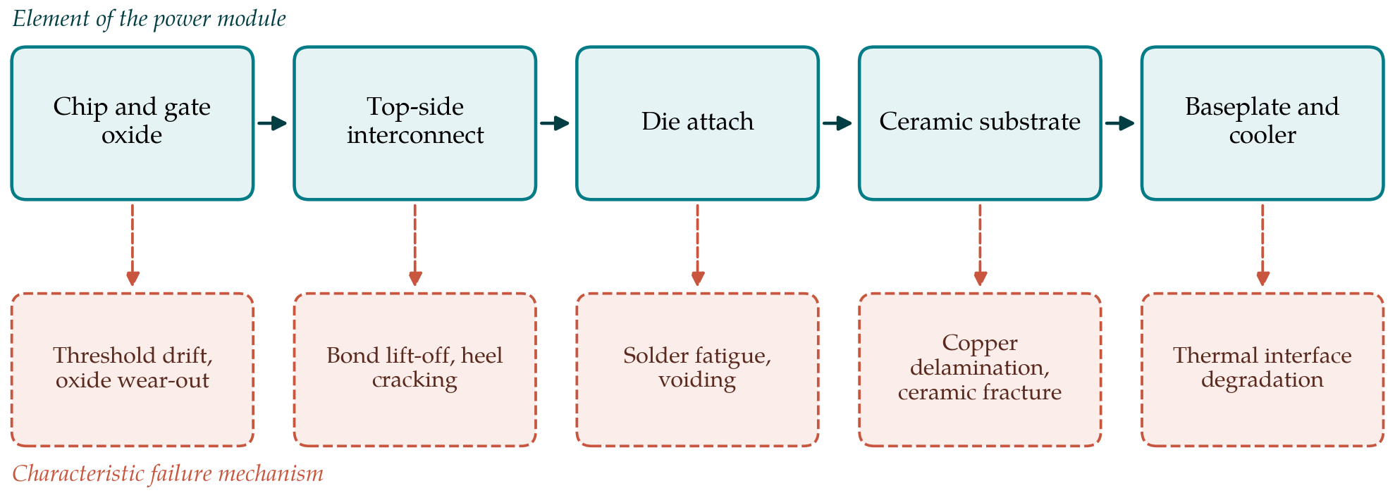
The reviews of Chen et al. (2017) and Lee et al. (2020) describe a consistent set of responses. In die attach, solder is giving way to sintered silver, whose melting point of 961 °C lies far above any operating temperature and whose thermal and electrical conductivities exceed those of solder alloys; Siow (2014) reviews its processing and remaining questions, such as porosity control and behaviour on different metallisations. On the top side, aluminium wires are being replaced by copper wires and ribbons, copper clips, or planar and flexible-foil interconnects that also remove heat from the upper face of the chip. For the substrate, silicon nitride joined by active metal brazing offers higher fracture toughness than alumina or aluminium nitride and tolerates the wider temperature swings.
Two further trends are electrical and thermal in motive. Wide-bandgap devices switch in tens of nanoseconds, and any inductance in the commutation loop converts the current slope into overshoot and ringing. Module layouts have accordingly moved towards laminated or stacked current paths, integrated decoupling capacitors and separate Kelvin source connections for the gate circuit (Chen et al., 2017). On the thermal side, direct liquid cooling of a pin-fin baseplate removes the thermal interface material, and double-sided cooling, made possible by planar interconnects, extracts heat from both faces of the chip. Transfer-moulded packages, which encapsulate the assembly in epoxy in place of silicone gel inside a frame, have become common in automotive modules (Reimers et al., 2019).
6. Qualification and Lifetime Assessment
Automotive components are qualified against agreed stress-test catalogues. Discrete devices follow AEC-Q101 (Automotive Electronics Council, 2021), and power modules for vehicle converters are commonly qualified to the ECPE guideline AQG 324, which has been extended with provisions specific to SiC (ECPE, 2021). Power cycling is central to both. The empirical lifetime relations in use descend from the work of Held et al. (1997) on IGBT modules for traction, which expressed the number of cycles to failure as a function of junction temperature swing and mean temperature.
Two difficulties attend the transfer of these methods. Lifetime models fitted to soldered, wire-bonded silicon modules cannot be assumed to hold for sintered, clip-bonded SiC modules, whose dominant failure site may have moved. And power cycling of a SiC MOSFET is complicated by the threshold drift described earlier, which disturbs the temperature-sensitive electrical parameter normally used to infer junction temperature during the test. Wang et al. (2013) argue more generally for a physics-of-failure approach in which lifetime is designed from mission profile and mechanism, not demonstrated afterwards by a fixed test list.
7. System-Level Consequences of Fast Switching
Reliability does not end at the module terminals. The steep voltage edges that reduce switching loss also travel down the motor cable. Morya et al. (2019) review the effects on the drive: reflected-wave overvoltage at the motor terminals, uneven voltage distribution across the first turns of the winding with attendant risk of partial discharge, bearing currents driven by common-mode voltage, and increased conducted and radiated electromagnetic interference. The close integration of inverter and motor in a vehicle shortens the cable and eases the first of these, but the others remain. In practice the switching speed of a traction inverter is often set below what the devices could achieve, which means that part of the theoretical loss advantage is traded for insulation life and electromagnetic compatibility.
8. Open Questions
Several matters are unsettled in the published record. Validated lifetime models for the new material combinations are scarce, and those that exist are mostly held by manufacturers. Accelerated tests apply regular cycles, whereas a vehicle imposes an irregular mixture of short and long, shallow and deep temperature excursions, and the rules for accumulating damage across such a mixture are not well established for sintered joints. The interaction of mechanisms, for example whether threshold drift alters current sharing between paralleled chips and thereby their thermal loading, has received little study. For GaN, the path to the traction inverter depends on higher-voltage devices or multilevel topologies and on packages able to exploit a lateral chip. Finally, condition monitoring in service, which would allow maintenance to be based on measured degradation, remains largely a research topic (Wang et al., 2013).
9. Conclusion
The literature presents wide-bandgap traction converters as a technology whose electrical case is made and whose reliability case is still being assembled. For SiC, the device-level concerns of oxide stability, bipolar degradation and short-circuit withstand are understood well enough to be managed by processing, screening and protection. The larger shift is in the package, where sintered joints, copper and planar interconnects, tougher substrates and double-sided cooling are displacing a construction optimised for silicon. Qualification practice is adapting, but lifetime prediction for the new material sets under real driving profiles rests on a thinner evidential base than designers had for the IGBT module, and that is where further published work would be most valuable.
Conflict of interest
To be declared by the author(s) before publication.
Funding
To be declared by the author(s) before publication.