1. Introduction
For two decades the principal answer to short-channel effects has been to bring more gate around the channel. The fin field-effect transistor, proposed as a self-aligned double-gate device by Hisamoto et al. (2000) and introduced in volume manufacturing as the tri-gate transistor at the 22 nm node (Auth et al., 2012), wrapped the gate over three sides of a narrow silicon fin. The gate-all-around (GAA) transistor completes the enclosure. In its manufacturable form, horizontal silicon nanosheets are stacked one above another and the gate stack fills the spaces between them (Loubet et al., 2017). A three-nanometre technology built on this multi-bridge-channel structure has been described by Bae et al. (2018).
Circuit designers meet a new transistor first through its model card and design rules. Its reliability reaches them later, as ageing models, current-density limits, self-heating rules and guard-bands, usually with little explanation of the physics behind them. That gap matters more with each generation, because the margins that once absorbed ageing have narrowed with the supply voltage, and because analogue and mixed-signal circuits stress devices in ways that digital qualification does not anticipate (Lewyn et al., 2009).
This review is written for those designers. It summarises the degradation mechanisms that the literature identifies as most affected by the change of geometry and translates each into the circuit behaviour it produces. It presents no new measurements and reproduces no foundry data.
2. Scope and Approach
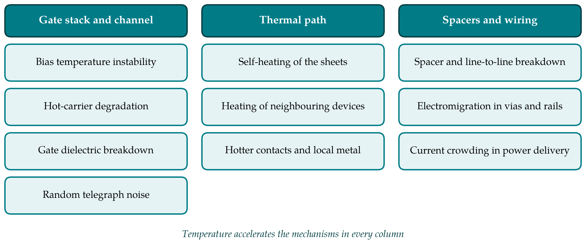
The article is a narrative review of the published literature on transistor and interconnect reliability, read from the standpoint of circuit design. The sources are foundational papers on each mechanism, review articles and monographs on reliability physics (McPherson, 2010), conference papers describing nanosheet technologies, and industry documents such as the JEDEC guide to failure mechanisms and models (JEDEC, 2016). No systematic search protocol was followed and no claim of completeness is made. Where the open literature on nanosheet devices is thin, the review says so and reasons from the better documented behaviour of fins, marking such reasoning as inference. Figure 1 groups the mechanisms covered by the part of the structure in which they originate.
3. From Fins to Nanosheets
Three structural features of the stacked nanosheet transistor bear on reliability. First, the channel is a thin slab of silicon surrounded on every side by gate dielectric and metal, connected to the outside only through its source and drain epitaxy. Second, the sheets are formed by growing alternating silicon and silicon-germanium layers and later etching the sacrificial layers away, after which the gate dielectric and work-function metals must be deposited inside gaps only a few nanometres tall, so the sheet spacing limits the thickness of the layers that set the threshold voltage. Third, an inner spacer separates the gate from the source and drain between sheets, and its quality controls both parasitic capacitance and the field across a very short dielectric path.
For the designer the visible change is that device width is no longer quantised in fins. Sheet width is a layout variable, so drive strength can be traded against capacitance and area in finer steps (Bae et al., 2018). The conducting surfaces also differ. A fin conducts mainly on its sidewalls, whereas a nanosheet conducts mainly on its top and bottom faces, with the sheet edges forming a smaller part of the perimeter. Further ahead, stacking n-type and p-type devices vertically in the complementary FET has been proposed to continue cell scaling (Ryckaert et al., 2018), and would add its own thermal and wiring constraints.
4. Bias Temperature Instability
Bias temperature instability (BTI) is the gradual shift of threshold voltage, with loss of drive current, in a transistor held in inversion at elevated temperature. The negative-bias form in p-channel devices was the dominant ageing concern of the silicon oxynitride era (Schroder and Babcock, 2003); the introduction of hafnium-based dielectrics added a positive-bias form in n-channel devices attributed to electron trapping in the high-permittivity layer. Two descriptions of the physics have competed. The reaction-diffusion framework attributes the shift to the breaking of silicon-hydrogen bonds at the interface and diffusion of the released species (Alam and Mahapatra, 2005). The defect-centric view attributes much of the shift, and all of its fast recovery, to charge capture and emission by oxide traps with widely distributed time constants (Grasser, 2012).
The distinction matters to designers through recovery and through statistics. Part of the shift relaxes soon after the stress is removed, so the degradation a circuit experiences depends on its duty cycle and on how recently a device was stressed. In a small device the shift is produced by a handful of traps, each contributing a discrete step whose size depends on where the trap sits relative to the current path. Kaczer et al. (2010) showed that the resulting distribution of threshold shifts across nominally identical devices is broad and skewed, so that the mean shift quoted in a qualification report understates what the worst transistors in a large array will suffer.
For nanosheets three points recur in the literature. Sheet corners and edges concentrate the oxide field locally. The constrained thickness of the work-function metal leaves less freedom to engineer the stack for each threshold flavour, so different threshold options may age differently. And because nanosheet channels run hot, the effective temperature for BTI in a switching circuit exceeds the average die temperature.
5. Hot-Carrier Degradation and Self-Heating
Hot-carrier degradation arises when carriers gain enough energy in the channel field to create interface states or become trapped near the drain. The classical lucky-electron picture of Hu et al. (1985) located the worst case at the gate bias of peak substrate current and was associated with less damage at higher temperature. In short-channel devices at low supply voltage the picture is widely reported to have changed: damage is driven by the cumulative action of many carriers of moderate energy, the worst case has moved towards the condition of full gate and drain bias, and degradation increases with temperature. Hot-carrier damage does not recover appreciably, so it accumulates with every switching event and with every hour an analogue device spends in saturation at high drain voltage.
Self-heating ties hot-carrier damage to geometry. Heat generated near the drain of a planar bulk transistor spreads directly into the silicon substrate. In a nanosheet the nearest heat paths run through the gate stack, whose dielectric layers conduct poorly, and along the thin sheet to the source and drain. Thin silicon films conduct heat far less well than bulk silicon because phonons scatter at the surfaces, an effect analysed for nanoscale transistors by Pop et al. (2006). The consequence, reported for fins and expected to be stronger for sheets, is a local temperature rise that depends on power density, on the number of adjacent active devices and on the switching activity.
The temperature rise matters twice. During operation it lowers mobility and shifts thresholds, which a device model that includes self-heating can capture. Over life it accelerates BTI and hot-carrier damage in the heated device and in its neighbours, and it warms the contacts and first metal layers above. For digital logic with low activity the average rise is small. For clock buffers, output drivers, oscillators and any analogue device carrying static current at high drain voltage, it can decide lifetime.
6. Time-Dependent Dielectric Breakdown
Time-dependent dielectric breakdown (TDDB) is the formation, under sustained field, of a conducting path through the gate dielectric. The percolation model of Degraeve et al. (1998) explains its statistics: defects generated at random positions eventually line up to bridge the dielectric, the time to breakdown follows a Weibull distribution, and the distribution scales with total gate area, so that a large circuit fails at its weakest device.
A gate that surrounds the channel has more dielectric area per unit of footprint, with corners where the field is locally higher. Of at least equal concern in scaled nodes is breakdown outside the gate dielectric proper: between gate and source-drain contact across the spacer, across the inner spacer between sheets, and between closely spaced metal lines in the low-permittivity dielectric of the lower interconnect levels. These paths are a few nanometres long and see the full supply or, in input-output and analogue circuits, more. Designers encounter them as voltage-dependent spacing rules and as limits on the voltage that may appear across adjacent nets.
7. Variability and Random Telegraph Noise
The undoped channels of fins and nanosheets removed most of the random dopant fluctuation that dominated threshold mismatch in planar bulk devices (Asenov, 1998). What remains comes from the granularity of the work-function metal, line-edge roughness of the gate, and variation in the dimensions of the channel body itself (Kuhn et al., 2011). In a nanosheet the relevant dimensions are sheet thickness, set by epitaxy, and sheet width and gate length, set by patterning and etch. Because thickness sets the degree of quantum confinement, variation in it moves the threshold voltage directly. The matching coefficient that an analogue designer uses therefore depends on sheet width in a way that has no equivalent in a process with quantised fins.
Random telegraph noise (RTN) is the time-domain signature of a single trap capturing and releasing a carrier (Kirton and Uren, 1989), and it is closely related to the recoverable part of BTI (Grasser, 2012). Its amplitude grows as gate area shrinks, since one trapped charge then controls a larger share of the channel. In static memory cells and in sense amplifiers RTN subtracts from margins that are already narrow at low supply voltage. In analogue circuits it appears as a low-frequency noise spectrum that departs from the smooth 1/f form, varies from device to device and cannot be predicted from an average noise model.
8. Electromigration in the Local Interconnect
Electromigration is the transport of metal atoms by the momentum of conduction electrons. Its dependence on current density and temperature is summarised in the empirical equation of Black (1969), in which lifetime falls as a power of current density and exponentially with temperature. Short segments benefit from the back-stress effect identified by Blech (1976), which can halt migration below a critical product of current density and length. Both relations are embedded in the current-density rules of every process (Lienig and Thiele, 2018).
Scaling tightens those rules from several directions. Local interconnect and vias have shrunk in cross-section faster than the currents they carry, the resistivity of narrow copper lines rises because of surface and grain-boundary scattering, and barrier and liner layers occupy a growing share of the trench. Self-heating adds to the Joule heating of the wire itself, so the temperature in Black's equation is that of a line sitting above hot transistors. Power delivery is affected most. Roadmaps anticipate buried power rails and delivery of supply current from the back of the wafer (IRDS, 2022), which relieves congestion on the front side but concentrates current in new via structures and changes the path by which heat leaves the device layer.
9. What This Means at the Circuit Level
Table 1 gathers the mechanisms reviewed above with the reason the GAA geometry alters each, the symptom seen in circuits and the first response open to the designer. The subsections that follow take the circuit classes in turn and then consider what ageing simulation can and cannot tell.
| Mechanism | Why the geometry alters it | Circuit symptom | First design response |
|---|---|---|---|
| Bias temperature instability | Few traps per device; constrained gate stack Kaczer et al., 2010 | Slower paths, offset drift, lost memory margin | Margin for the tail; matched stress on matched devices |
| Hot-carrier degradation | Now worsens with temperature; channels run hot | Falling drive and gain in saturated devices | Limit drain voltage by stacking |
| Self-heating | Sheets enclosed by poor heat conductors Pop et al., 2006 | Local hot spots that speed other mechanisms | Spread current over more or wider sheets |
| Dielectric breakdown | More dielectric area; very short spacer paths | Added leakage and noise, then failure | Respect voltage-dependent spacing; avoid overdrive |
| Variability | Sheet dimensions replace dopants as the source | Mismatch that depends on sheet width | Size for matching; calibrate |
| Random telegraph noise | One trap controls more of a small channel | Irregular low-frequency noise; margin loss | Increase gate area where noise matters |
| Electromigration | Narrow hot lines; new power-rail structures | Rising resistance, then open circuits | Widen lines, add vias, check average and peak current |
9.1. Digital logic and memory
Digital design absorbs ageing through guard-bands: timing is signed off with libraries characterised for aged devices, or with a frequency or voltage margin. BTI slows p-channel and n-channel devices according to the fraction of time each spends in inversion, so paths that idle in one state age asymmetrically. The statistical character of BTI and RTN in small devices means that the margin must cover the tail of the distribution and not its mean, which is the practical message of the defect-centric work (Kaczer et al., 2010).
9.2. Analogue and mixed-signal circuits
Analogue circuits are exposed differently. They rely on matching, and a matched pair whose two halves see different bias histories acquires an offset that was absent at time zero. A comparator input pair held at a large differential voltage is the usual example. Bias networks and power-down states therefore deserve the same scrutiny as normal operation, because a device can be stressed hardest when its circuit is nominally off. Devices held in saturation at high drain voltage accumulate hot-carrier damage continuously.
The responses are established and are set out in the analogue reliability literature (Maricau and Gielen, 2013): limit the voltages across individual devices by stacking, keep matched devices under matched stress in every operating mode, spread current over more or wider sheets to reduce self-heating, calibrate or chop to remove drifting offsets, and place the most thermally active devices away from precision ones.
9.3. Ageing simulation and its limits
The Berkeley tools of Tu et al. (1993) established the pattern still used in ageing flows: simulate the fresh circuit, compute the stress on each device from its waveforms, update the device parameters, and simulate again. The pattern is sound, but its results are only as good as the stress models, and several features of scaled devices strain them. Recovery makes the result depend on the choice of stress waveform. Self-heating couples devices that the netlist shows as independent. Average-shift models miss the spread from device to device. A designer should therefore read an aged simulation as a ranking of which devices are at risk and not as a prediction of the shift each will show.
10. Gaps and Future Work
Several questions are not settled in the open literature. Most published reliability data on nanosheets come from device-level test structures under constant stress, and there is little public evidence on how ageing accumulates under realistic circuit waveforms with self-heating included. How the multiple threshold-voltage options of a nanosheet process differ in BTI, given the constraints on the gate stack between sheets, is documented only in part, as is the effect of sheet width on each mechanism.
Looking further ahead, backside power delivery and stacked complementary devices will change thermal paths and local current densities again, and the reliability consequences for analogue and input-output circuits, which use higher voltages than core logic, have received less attention than those for logic cells. Compact, statistically aware ageing models that include self-heating coupling and run on circuits of practical size also remain a research topic, and without them designers must rely on conservative rules of uncertain cost.
11. Conclusion
Gate-all-around transistors improve the switch and complicate its ageing. The mechanisms are familiar from earlier generations, but the geometry concentrates heat, shrinks the number of defects per device to the point where statistics dominate, and shortens every dielectric path around the gate. For circuit designers the working conclusions are to treat local temperature as a design variable, to examine stress in every operating mode including power-down, to design for the tail of the ageing distribution, and to regard ageing simulation as guidance. The open literature leaves real gaps, particularly for analogue and mixed-signal circuits.
Conflict of interest
To be declared by the author(s) before publication.
Funding
To be declared by the author(s) before publication.