1. Introduction
A filter bank splits a signal into sub-bands so that each can be processed, measured or discarded separately. When the bands are fixed, the design problem is well understood and the theory is laid out in standard texts (Vaidyanathan, 1993). The harder case is a bank whose bands must change in service. A radio front end built on the software radio principle is expected to serve standards with different channel spacings (Mitola, 1995), and its channeliser has to follow. A hearing instrument fits its bands to the user's audiogram. In both, the equipment runs from a battery.
Field-programmable gate arrays are a natural platform for prototyping such banks, and the smallest families, built on flash or low-leakage memory cells, have static power low enough to remain in a portable product. They are also small. Programmable logic pays a substantial penalty in area and power relative to cell-based design (Kuon and Rose, 2007), and a low-power device offers few logic cells and very few hardened multipliers. This note considers how a reconfigurable filter bank can be arranged to fit within those limits. It is a commentary on design choices drawn from the published literature and presents no experimental results.
2. Routes to Reconfigurability
Four approaches recur in the literature, and they differ in what is shared between bands and in what has to change when the band plan changes. Table 1 sets them side by side, together with the plain alternative of storing a separate coefficient set for every band plan.
| Approach | What reconfigures | Main resource demand | Limitation |
|---|---|---|---|
| Modulated polyphase bank | Number of bands; prototype coefficients | One prototype filter and a transform | Bands uniform unless outputs are merged |
| Coefficient decimation | Decimation factor applied to one coefficient set | Multiplexers on the tap selection | Stopband attenuation falls as the factor rises |
| Frequency-response masking | Interpolation factor and masking filters | Long delay lines in memory | High group delay |
| Cascaded integrator-comb | Rate change factor | Adders and registers only | Passband droop; needs compensation |
| Stored coefficient sets | Whole coefficient set swapped per band plan | Memory for every stored set | Memory grows with the number of plans |
In a modulated bank, a single low-pass prototype is shifted in frequency to form every band. With polyphase decomposition the prototype is computed once at the low output rate and a discrete Fourier or cosine transform performs the modulation (Bellanger et al., 1976), an arrangement that has become the standard channeliser for communication receivers (harris et al., 2003). The cost per band is low, but the bands are uniform. Unequal bands are obtained by merging adjacent outputs or by changing the prototype.
Coefficient decimation obtains several responses from one stored filter. Keeping every M-th coefficient and replacing the others with zeros produces a multi-band response, and discarding the others altogether widens the passband, so that the integer M becomes the control (Mahesh and Vinod, 2008). The same authors built low-complexity uniform and non-uniform channelisers on the idea (Mahesh and Vinod, 2011). Frequency-response masking, due to Lim (1986), reaches sharp transitions with sparse coefficients by interpolating a model filter and removing the unwanted images with masking filters. Cascaded integrator-comb filters use no multipliers at all (Hogenauer, 1981) and suit the first stage of rate reduction more than band selection.
3. An Implementation Pattern for Small Devices
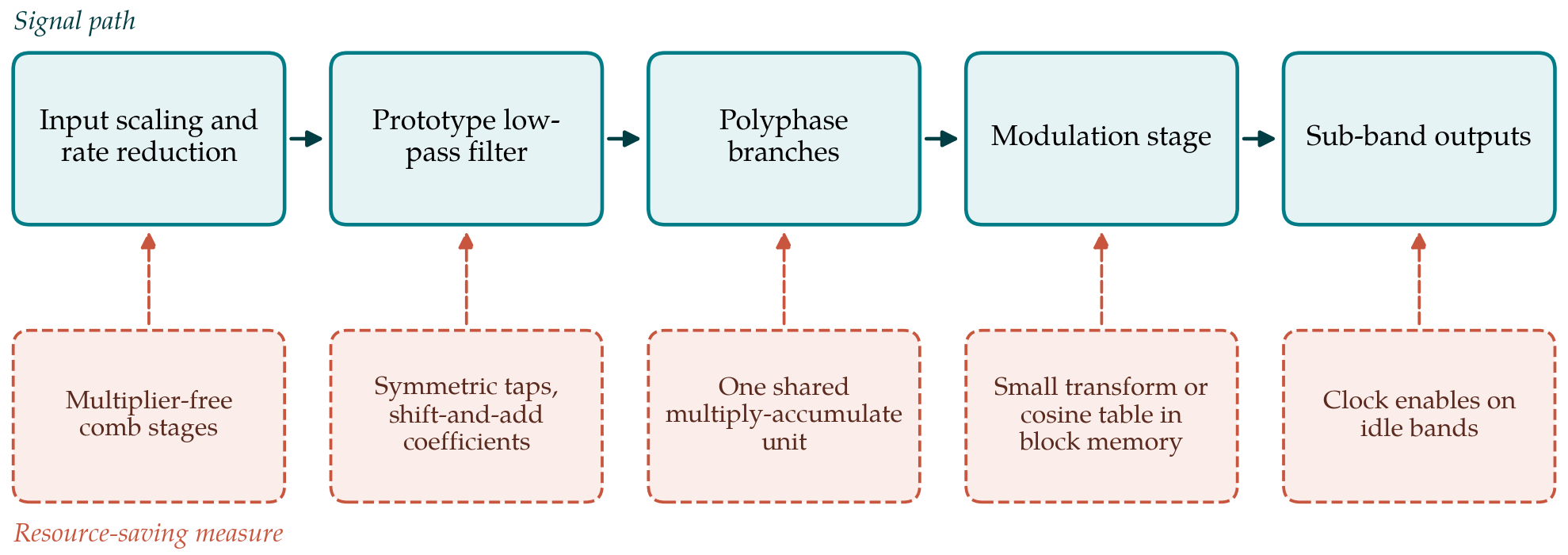
The reasoning that follows leads to the arrangement in Figure 1, in which each stage of the signal path is paired with the measure that keeps its cost down. The starting point is that hardened multipliers are the scarcest resource and that the sample rates of audio and narrowband radio are far below the clock rate a gate array can sustain. Arithmetic should therefore be shared in time. A polyphase prototype with N taps needs N multiplications per output frame, and at a low output rate one multiply-accumulate unit, cycling through the taps, can perform them all. Coefficients and the sample delay line are held in block memory, which small devices provide in more generous measure than multipliers.
Where even one multiplier is unavailable, two older techniques apply. Distributed arithmetic replaces the multiplier with a look-up table addressed by one bit of every input sample and an accumulator, which maps directly onto the look-up tables of programmable logic (White, 1989). Its table depends on the coefficients, so for a reconfigurable filter the table has to live in writable memory. The alternative is to restrict coefficients to sums of a few signed powers of two and build the products from shifts and adders with shared sub-expressions (Dempster and Macleod, 1995). This gives the smallest fixed filter but hard-wires the coefficients, and it is best kept for the parts of the bank that never change, such as a compensation filter after an integrator-comb stage. Practical guidance on both is collected by Meyer-Baese (2014).
Reconfiguration should be a matter of writing parameters. Loading a new bitstream interrupts the signal and, on flash-based devices, is slow. If the band plan is expressed as a coefficient set in memory, a tap count, a decimation factor M and a table saying which transform outputs are merged, a small controller can change it between frames. Coefficient decimation fits this scheme well, since a new response needs only a different address stride through the same memory. The polyphase structure fits it too, provided the transform size is fixed and unused outputs are simply not computed.
Dynamic power in programmable logic is dominated by the clock network and by switching in the routing. Three habits follow. Sections that are idle in the current band plan should have their clock enables held low, so that their registers do not toggle. Word lengths should be set stage by stage from the required dynamic range and not left at a uniform width, because every surplus bit is carried through every adder and memory word. The fast clock that drives the shared arithmetic should be no faster than the tap count requires.
Memory organisation needs some care as well. The delay line is most economically built as a circular buffer in a block memory with a moving write pointer, so that no data are shifted, and the coefficient memory is read in step with it. Where the prototype has linear phase its coefficients are symmetric, and half of them need be stored; a pre-adder that sums the two samples sharing a coefficient then halves the number of multiplications per frame. Both measures are standard, and both reduce the clock rate required of the shared arithmetic unit, which is what the power budget ultimately depends on.
4. Where the Pattern Is Likely to Fail
Three limits should be expected. Time-multiplexing breaks down as the sample rate rises: once the product of tap count and output rate approaches the achievable clock frequency, a second arithmetic unit is needed and the area advantage erodes. Coefficient decimation degrades the stopband as the factor increases, because the retained coefficients sample the prototype response more coarsely, so the prototype must be over-designed for the largest factor in use. Fixed-point effects are sharper in a shared datapath as well. A single accumulator width has to serve every band plan, and the guard bits that suffice for a narrow band may overflow for a wide one.
5. What a Full Report Should Disclose
Published accounts of filter banks on gate arrays are hard to compare, because resource counts are given without the conditions that produced them. A report of an implementation along these lines would be more useful if it stated the device and tool version; the look-up tables, registers, memory blocks and hardened multipliers used; the sample rate and clock rate; the word lengths at each stage; and the prototype specification, including passband ripple and stopband attenuation for every supported configuration. Power should be measured on the board, separated into static and dynamic parts, and accompanied by the input signal used, since tool estimates depend strongly on assumed switching activity. The time taken to change configuration, and whether the output is interrupted, should be given as well.
6. Conclusion
A reconfigurable filter bank can be made compact enough for a low-power gate array by sharing one prototype among the bands, computing it with time-multiplexed arithmetic, keeping coefficients in block memory and changing the band plan through parameters. The approach trades throughput for area, and it suits audio and narrowband applications better than wideband ones. This note has given the reasoning and the expected limits. Measured implementations, reported with the detail listed above, are needed to show how far the pattern holds on particular devices.
Conflict of interest
To be declared by the author(s) before publication.
Funding
To be declared by the author(s) before publication.