1. Introduction
The idea that students should design chips and receive them back from a foundry is as old as structured VLSI design. The methodology of Mead and Conway (1980) separated design from fabrication through simple scalable rules, the multi-project wafer spread mask costs across many designs, and the MOSIS service made the arrangement routine for universities in the United States (Tomovich, 1988; Conway, 2012). What did not become routine was access. Foundry design kits stayed behind non-disclosure agreements, commercial tools required licences and administration, and many departments, particularly smaller ones, taught integrated circuit design entirely in simulation.
Two developments have changed this for mature nodes. Predictive kits such as FreePDK (Stine et al., 2007) and ASAP7 (Clark et al., 2016) had long let students practise physical design without restrictions, but they describe processes that cannot be manufactured. The release in 2020 of an open, manufacturable 130 nm kit by SkyWater Technology with Google, described by Ansell and Saligane (2020), closed that gap and was followed by open kits from other foundries. In parallel the OpenROAD project produced an autonomous open-source digital layout flow (Ajayi et al., 2019), packaged for the open kit as OpenLane (Shalan and Edwards, 2020).
For purely digital projects the path is now well trodden. For mixed-signal projects it is not, because the analogue portion is drawn by hand with a different set of tools, and joining the two halves is where a project is most exposed to error. This article proposes a staged flow for mixed-signal tape-outs in a university course using only open-source software. It describes a method and does not report the results of teaching with it.
2. Background
The proposal rests on three things an instructor needs to know before planning such a course: which open tool does which job, how silicon is reached, and why a mixed-signal chip asks more of the flow than a digital one.
2.1. Open tools for each task
The open toolchain mirrors the commercial one stage for stage. Circuit simulation rests on SPICE, first described by Nagel and Pederson (1973) and maintained today as ngspice; schematics are commonly drawn in Xschem. Full-custom layout, design rule checking and parasitic extraction are done in Magic, a tool whose lineage goes back to Berkeley in the 1980s (Ousterhout et al., 1984), with KLayout widely used for viewing and for a second design rule check, and Netgen for comparison of layout against schematic (LVS). On the digital side Yosys performs logic synthesis (Wolf and Glaser, 2013) and OpenROAD performs floorplanning, placement, clock tree synthesis and routing.
2.2. Routes to silicon
Access to silicon comes through shared-wafer programmes. Some provide a fixed harness, a padframe with a management processor and a user area into which the project is placed, which removes input-output design from the task set to students. Others divide a single user area among many small designs; Tiny Tapeout, described by Venn (2024), follows this model. Accounts of chips fabricated through open flows are given by Edwards et al. (2021). Programmes, prices and schedules change, and an instructor must confirm what is on offer before fixing a syllabus.
2.3. Why mixed-signal is harder
A digital block is described once, in a hardware description language, and every later representation is derived from it by tools. An analogue block has two hand-made descriptions, schematic and layout, that must be proved equivalent, and its performance depends on layout details such as matching, symmetry and parasitic capacitance that no netlist captures until extraction (Hastings, 2006; Baker, 2019). At the top level the two worlds meet across signals that the digital tools treat as logic values and the analogue simulator treats as voltages. Supplies, substrate ties and guard rings must be planned for both. Verification of the whole chip in SPICE is too slow, and in a digital simulator it is blind to the analogue behaviour, so some form of behavioural modelling is needed (Kundert and Zinke, 2004).
3. The Proposed Flow
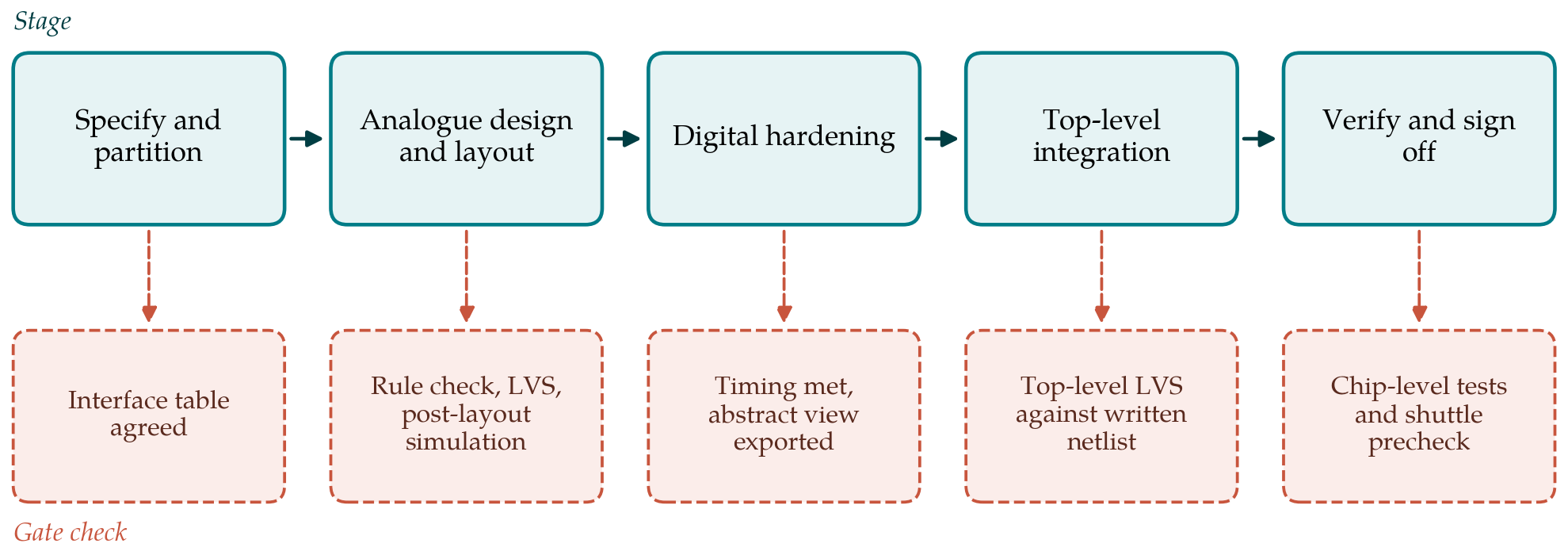
The flow has seven stages, each ending in a gate: a deliverable that must exist and pass a stated check before the team moves on. Table 1 lists the stages with the tools and the gate for each, and Figure 1 pairs the main design stages with the check that closes each of them. The gates are the teaching device. They give the instructor fixed points at which to review work, and they guard against the situation in which a team learns in the last week that its analogue layout does not match its schematic. The flow is proposed here and has not been validated in a course.
| Stage | Open tools | Gate deliverable |
|---|---|---|
| 1. Specify and partition | Document and block diagram | Pin list, interface table and outline of the test plan |
| 2. Analogue schematic | Xschem, ngspice | Corner simulations meeting the block specification, with testbench |
| 3. Analogue layout | Magic, KLayout, Netgen | Clean rule check and LVS; post-layout simulation passes |
| 4. Digital hardening | Yosys and OpenROAD through OpenLane | Timing-clean macro with netlist and abstract view |
| 5. Top-level integration | Magic or KLayout, Netgen | Top-level LVS match against a hand-written netlist |
| 6. Verification and sign-off | ngspice, Verilog simulator | Chip-level tests pass; shuttle precheck clean |
| 7. Bring-up plan | Board design tool, scripts | Test board schematic, script and measurement table |
3.1. Stage 1: Specify and partition
The team writes a one-page specification and a block diagram, and then draws the line between analogue and digital. The rule of thumb for a first project is to keep the analogue part small and well understood, for instance a comparator, a resistor-string converter or a ring oscillator with a tuning input, and to move as much function as possible, such as calibration, sequencing and serial communication, into logic. The output is an interface table listing every signal that crosses the boundary with its direction, voltage domain and meaning, and a pin list that fits the chosen shuttle. Test access is decided here: any analogue node that will need to be observed must be given a path to a pad through a buffer or an analogue multiplexer, because it cannot be added later.
3.2. Stage 2: Analogue schematic design
Each analogue block is captured in Xschem and simulated in ngspice with the device models of the kit. Students size devices from hand analysis as taught in standard texts (Baker, 2019), then check the design across the process corners, supply range and temperature range that the kit provides, and run Monte Carlo analysis where the kit supports mismatch models. The gate is a short report showing that the block meets its specification over those conditions, with a testbench that is kept under version control. Requiring the testbench, and not just the plots, pays off at stage 3, where the same testbench is rerun on the extracted netlist.
3.3. Stage 3: Analogue layout and extraction
Layout is drawn in Magic, whose interactive design rule checking shows violations as they are made, which suits beginners. The parameterised device generators of the kit provide transistors, resistors and capacitors; students place and wire them with attention to the matching practices of Hastings (2006): common-centroid or interdigitated arrangement of matched devices, dummy devices at the ends of arrays, identical orientation and symmetrical routing. The gate has three parts. The layout passes the full design rule deck, including a second run in KLayout because the two tools implement the rules independently. Netgen reports a match between the extracted layout and the schematic. And the stage 2 testbench, run on the netlist with extracted parasitics, still meets the specification.
3.4. Stage 4: Digital hardening
The digital part is written in Verilog, simulated with an open simulator such as Icarus Verilog or Verilator, and hardened into a macro with OpenLane, which runs synthesis, placement, clock tree synthesis, routing and static timing analysis from a configuration file (Shalan and Edwards, 2020). A course can treat the flow as a black box or open it up as time allows. The gate is a macro with no timing or rule violations, delivered with its layout, its gate-level netlist and an abstract view giving its outline and pin positions. Pin positions should be fixed by the top-level floorplan and not left to the tool.
3.5. Stage 5: Top-level integration
Integration is where a mixed-signal project differs most from a digital one. A top-level floorplan places the analogue blocks, the digital macro and any harness, with analogue blocks kept away from switching logic and given their own supply and ground pads where the pin budget allows. Guard rings and, where the process offers it, deep n-well isolation limit substrate coupling. Connections between blocks are drawn by hand or with a simple router. The essential discipline is a hand-written top-level netlist, in SPICE or structural Verilog, that states what should be connected to what. The gate is a match between the extracted top-level layout and that netlist, with every block treated first as a black box and then flattened.
3.6. Stage 6: Mixed-signal verification and sign-off
Chip-level verification needs a model of each half that the simulator of the other half can use. Two routes are available with open tools. In the first, each analogue block is given a simple behavioural model in Verilog, with real-valued quantities where needed, so that the full chip can be exercised in the digital simulator; the model is trusted only as far as it has been compared with the SPICE simulation of the block. In the second, the digital logic is brought into ngspice through its event-driven mixed-mode capability, which is accurate at the boundary but slow. A sensible gate asks for the first route for functional tests and the second for one or two critical interactions, such as the sampling instant of a converter. Sign-off repeats the full rule checks on the merged layout and runs whatever precheck the shuttle requires.
3.7. Stage 7: Bring-up plan
Silicon returns months after submission, usually after the course has ended. The final gate is therefore a bring-up plan produced before tape-out: a schematic for a test board or a list of the bench instruments needed, a script that exercises the chip through its serial interface, and a table of the measurements that will be compared with simulation. Writing the plan before submission is a last check on test access while there is still time to add it, and it lets a later cohort or a project student carry out the measurements.
4. Fitting the Flow to a Semester
A semester of about fourteen weeks is short for seven stages, and the flow assumes that some things are fixed in advance by the instructor. The shuttle, the harness and the padframe are chosen before the course starts. A working reference design, taken through every stage, is given to the students in the first week so that tool installation problems appear early; container images of the toolchain reduce the time lost to set-up. Teams of three or four allow one member to own the digital macro while the others share the analogue blocks, and the interface table of stage 1 is the contract between them.
The stages overlap in time. Stages 2 and 4 can run in parallel once stage 1 is signed, and an early, empty version of the top level with dummy blocks of the right size can be taken through stage 5 by the middle of the term, so that integration problems are found before the real blocks arrive. The educational argument for the whole exercise is the familiar one for learning through concrete experience and reflection (Kolb, 1984) and for active methods in engineering teaching (Prince, 2004). Where tape-out dates do not align with the calendar, the gates can still be assessed, and fabrication treated as a consequence of the course and not as a condition of passing it.
5. Limitations and What Remains to Be Shown
This article sets out a flow and the reasoning for it. It does not report on a cohort of students who followed it, and no claim is made about learning outcomes or first-silicon success. Three things would need to be shown. The first is that the gates catch the errors they are meant to catch, which could be examined by recording at which stage each defect in student projects is found. The second is that the workload fits a semester for students without prior layout experience. The third is that chips made this way work, which requires measurement of returned silicon against the bring-up plan.
The open tools also have limits that an instructor should state openly. Parasitic extraction in the open flow is less thoroughly qualified against silicon than commercial sign-off extraction, the device models of open kits are less mature at the extremes of bias and temperature, and analogue placement and routing are manual. Open kits exist only for mature nodes. None of this prevents the teaching of sound practice, but students who go on to industry will meet different tools, and the course should present the flow as an instance of general principles.
6. Conclusion
Open kits and open tools make it possible for a university course to end in a mixed-signal chip and not only a simulation. The seven-stage flow proposed here assigns an open tool and a checkable deliverable to each stage and puts its weight on the points where analogue and digital meet: the interface table, the top-level netlist and the behavioural models. Its merit as a teaching method remains to be established by those who run it with students and measure what comes back.
Conflict of interest
To be declared by the author(s) before publication.
Funding
To be declared by the author(s) before publication.