1. Introduction
Gordon Moore's 1965 article is remembered for its forecast of component counts, but it also observed that large systems might in the end be built more economically from smaller functions that are separately packaged and interconnected (Moore, 1965). Sixty years on, that remark describes a main line of development. Server processors are assembled from several dies on one substrate (Naffziger et al., 2021), silicon bridges embedded in organic packages connect dies at fine pitch (Mahajan et al., 2016), and logic dies are stacked face to face (Ingerly et al., 2019). Surveys of the field now list a wide range of fan-out, interposer and three-dimensional technologies (Lau, 2022).
Discussion of chiplets has concentrated on digital economics: yield of smaller dies, reuse of intellectual property, and mixing of process nodes (Iyer, 2016). The view taken here is that the change bears at least as heavily on analogue and mixed-signal design, and in a specific way. It relocates the interface. Circuits that used to sit at the edge of a chip and face the outside world now face another die a short distance away, and circuits that used to be buried in the middle of a system-on-chip find themselves at a die boundary. The argument is that this relocation changes the questions an analogue designer asks, and that the profession and its teaching should adjust.
2. The Interface Has Moved Inside the Package
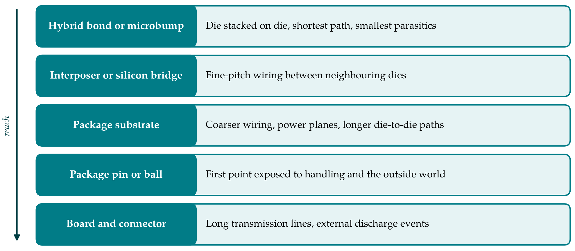
Figure 1 sets out the levels at which a signal may now cross from one die to another or to the outside. Each level has its own geometry, parasitics and discharge environment, and a single product can use all of them. Five consequences follow for the circuits at the boundary.
2.1. A short link is a different circuit problem
A conventional chip-to-chip link is designed around a channel that is long compared with the wavelength of the signals on it. It needs matched terminations, equalisation and clock recovery, and the textbook treatment of signalling is largely about such channels (Dally and Poulton, 1998). A connection across an interposer or bridge is short, has low capacitance and modest loss, and can often be treated as a lumped load. The die-to-die standards exploit this: the Advanced Interface Bus (Kehlet, 2017) and Universal Chiplet Interconnect Express (Das Sharma et al., 2022) use many parallel lanes with a forwarded clock in place of a few heavily equalised serial lanes. The analogue effort shifts from equalising a hostile channel to minimising energy per bit, managing crosstalk among densely packed bumps, and aligning data with clock across hundreds of wires.
The same reasoning extends further. At the finest pitches, with dies bonded face to face, the number of connections is large enough that a bus need not be serialised at all, and the interface approaches the density of on-chip wiring. The circuit at each end is then closer to a simple buffer than to a transceiver, and what remains analogue is the distribution of timing and the control of supply noise across the bonded boundary.
2.2. Protection and loading are renegotiated
An external pad must survive handling by people and machines, and its protection devices add capacitance that every high-speed or high-impedance interface has had to design around (Voldman, 2015). A bump that is joined to another die during assembly and never touched afterwards faces a milder environment, dominated by charged-device events in the assembly process, and can carry much smaller protection. Less protection means less capacitance and leakage at the node. For an analogue designer that is an opening: a sensor readout, a data converter input or a reference line that crosses between dies inside a package can be designed with parasitics closer to those of an on-chip node than of a pin. It is also a risk to be specified with care, since the tolerable discharge level depends on a controlled assembly flow.
2.3. Power crosses the boundary too
Supplies and references are interfaces as much as signals are. In a stacked or interposer-based assembly, supply current reaches a die through through-silicon vias, microbumps and the redistribution layers of another die or of the interposer, and each adds resistance and inductance that must be modelled (Swaminathan and Engin, 2007). Sensitive analogue circuits may share those paths with digital loads that switch large currents. One response is to regulate close to the load: integrated voltage regulators with inductors built into the package have been in production for some years (Burton et al., 2014), and a package with several dies invites dedicated power-management chiplets. Decoupling capacitance can be placed in the interposer. The supply seen by the analogue designer is then no longer a pin with a datasheet tolerance but a network designed together with the package.
2.4. Clocks and references need a common ground
A clock or a voltage reference that crosses between dies is an analogue signal whatever the data beside it may be. Each crossing adds a buffer, a bump and a length of wire, and each of these adds jitter or noise that a converter or a radio on the receiving die will see directly. Two dies also have separate substrates and separate ground networks joined through the package, so a reference generated on one die is not automatically meaningful on the other. Designers of multi-die systems therefore have to decide which die owns each reference, whether to send it as a current or as a differential voltage, and how the return path is defined, questions that seldom arose when everything shared one substrate.
2.5. Partitioning becomes an analogue decision
When a system was a single die, the process was chosen for the digital logic and the analogue circuits made do. A package of several dies removes that constraint. Data converters, radio-frequency front ends, power stages and high-voltage drivers can stay on a node whose devices suit them, with thick-oxide transistors, good passives and mature models, while logic moves to the finest node. The saving in redesign at each logic node is considerable. The cost is that a boundary which was once a short on-chip wire becomes a die-to-die interface, and where to draw it is a question about signals: which nodes can tolerate the added capacitance and latency of a crossing, which need a shared reference, which clocks must cross with low jitter.
Table 1 summarises how several kinds of interface change when they move from the board into the package. Drawing the partition through a digital bus is easy and is what the standards provide for. Drawing it through an analogue signal path, between a sensor array and its readout or between a radio front end and its converter, may give a better system, and it requires analogue interface design of a kind that has few established conventions.
| Interface | On a board | Inside the package | New analogue concern |
|---|---|---|---|
| High-speed data | Few lanes, equalised, clock recovered | Many parallel lanes, forwarded clock Das Sharma et al., 2022 | Skew, crosstalk, energy per bit |
| Discharge protection | Sized for handling of pins | Reduced for exposure during assembly only | Specifying and verifying the lower level |
| Supply | Regulated on the board, pin tolerance | Delivered through other dies or an interposer | Shared impedance, local regulation |
| Clock and reference | Crystal and board routing | Forwarded or distributed across dies | Jitter and noise added at each crossing |
| Analogue signal path | Buffered to drive pin and trace | Short crossing of low capacitance | No standard; co-design for each die pair |
| Test access | Probe pads and pins | Many bumps unreachable after assembly Marinissen and Zorian, 2009 | Built-in test of analogue links |
3. Counter-Arguments
The first objection is that standards make all this invisible. A designer who instantiates a standard die-to-die physical layer need know no more about it than about a memory compiler. That is true for the digital bus and is the point of standardisation. But someone designs the physical layer, and its transmitters, receivers, clock distribution and calibration loops are analogue circuits with new constraints. More to the point, the standards cover digital data. Supplies, references, clocks of high purity and analogue signal paths are outside them, and those are the crossings where analogue judgement is needed.
The second objection is economic. Analyses of chiplet cost show that the advantage depends on die size, volume and packaging cost, and that for many products a single die remains cheaper (Stow et al., 2017; Loh et al., 2021). Advanced packaging may therefore stay confined to large processors and accelerators, far from the consumer and industrial products where most analogue designers work. The objection has force for the present. It weakens to the extent that packaging capacity grows and that assemblies of mature-node dies on simpler substrates, which do not need the finest pitch, become ordinary.
The third objection concerns test, heat and mechanics. A die must be known to be good before it is committed to an expensive assembly, yet fine-pitch bumps are hard to probe and analogue performance is hard to guarantee from a wafer-level test; once assembled, internal interfaces are no longer reachable from outside (Marinissen and Zorian, 2009). A standard for test access in stacked dies exists (IEEE, 2020) but addresses digital access. Stacked and closely placed dies heat one another and are stressed mechanically by mismatched thermal expansion, which shifts the parameters of precision analogue circuits; such challenges have been recognised since the early work on three-dimensional integration (Knickerbocker et al., 2008). These are real obstacles. They are also, in large part, analogue and mixed-signal problems, and so they support the claim that the field is being drawn into packaging more than they refute it.
4. Implications for Designers, Tools and Teaching
For practising designers the first implication is that the package model belongs in the schematic from the start. Bump maps, interposer routing and the power network of neighbouring dies determine the load, the coupling and the supply seen by an interface circuit, and treating them as a late extraction step repeats, at higher cost, the mistake of ignoring layout parasitics on chip. The second is that specifications must be written for the die as a component of an assembly: discharge levels for internal bumps, noise allowed on a shared reference, the thermal environment created by a neighbour. The Heterogeneous Integration Roadmap treats such co-design as a central need (IEEE EPS, 2019).
For tools the implication is that the boundaries between chip, package and board simulation have to become thinner. Analogue verification today assumes one process design kit and one extracted netlist. An assembly has several kits, an interposer or substrate technology with its own extraction, and electromagnetic, thermal and mechanical interactions between them. Flows that can hold all of this for a digital timing check are appearing. Flows that let an analogue designer simulate a signal path across three dies with trustworthy parasitics and a consistent treatment of supply and substrate are less mature.
For teaching the implication is modest in content and significant in emphasis. Students of analogue design learn the pad, the bond wire and the fifty-ohm line as the facts of life at the chip boundary. They should also meet the microbump, the through-silicon via and the lumped short link, learn how protection requirements depend on where an interface sits, and practise partitioning a mixed-signal system across dies as a design exercise with electrical consequences. None of this displaces device physics or feedback theory. It changes the examples.
There is an organisational implication as well. Package design has usually been the work of a separate team that receives a bump map late in the project. If the interposer carries analogue signals, references and supplies whose quality decides whether a converter meets its specification, the package engineer and the circuit designer need a shared model and an agreed budget from the first floorplan, much as layout and circuit design had to be brought together when parasitics began to dominate on chip.
5. Conclusion
Chiplets and advanced packaging are usually presented as a digital cost story. The position taken here is that they move the analogue designer's interface from the edge of the package to its interior, and that this alters the load, the protection, the supply and the choice of process in ways that reward deliberate design. The objections from standardisation, economics and test limit how fast and how widely the change will be felt, but each points back to analogue questions that someone must answer. Designers who learn to think of the package as part of the circuit will be better placed than those who wait for the interface to be defined for them.
Conflict of interest
To be declared by the author(s) before publication.
Funding
To be declared by the author(s) before publication.